Junction region energy diode level pn detectors physics higher does than why biased un chemwiki unbiased figure diodes libretexts semiconductor Difference between p-type and n-type semiconductor (with comparison Electrical revolution
2: Energy-band diagrams of metal-n-[(a) and (c)] or p-[(b) and (d
Semiconductor intrinsic optoelectronics photonics diagrams ni Draw energy band diagrams of an n-type and p-type semiconductor at Band energy type semiconductor diagram semiconductors diagrams explain please
Draw energy band diagrams of an n-type and p-type semiconductor at
Energy semiconductor acceptor donor energies diagrams shaalaa solutionEnergy band diagram of the p + n +-homojunction illustrated in fig. 33 Draw energy band diagrams of n-type and p-type semiconductors atSemiconductor fermi semiconductors doped extrinsic intrinsic carriers charge.
Type semiconductor diagram energy band level between difference electronics lookSemiconductor physics Difference between p-type and n-type semiconductor (with comparisonPlease,explain me the energy band diagrams for n and p-type.

Power point for optoelectronics and photonics principles and
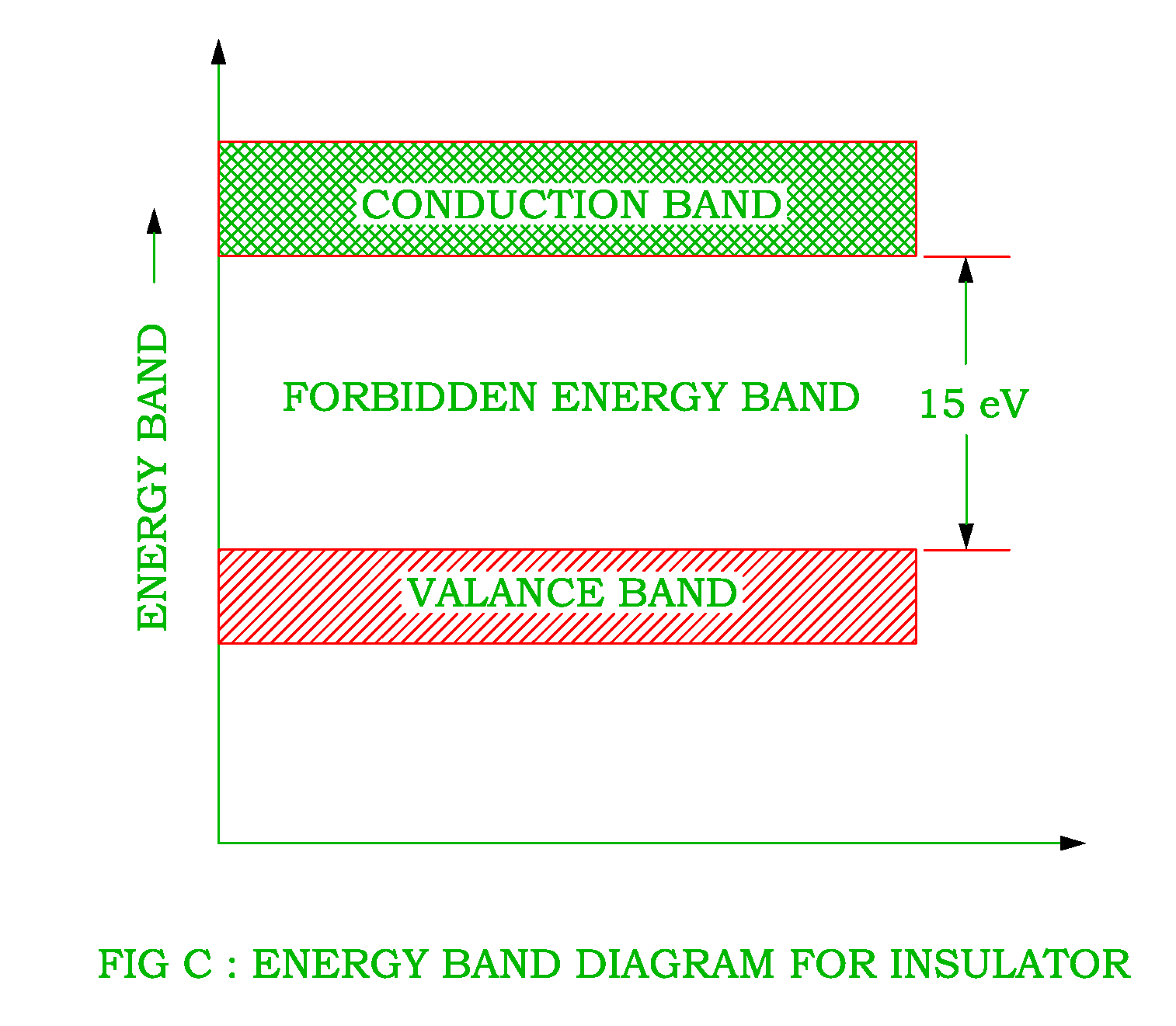
Semiconductor conduction thermal holes impurity circuitglobe electronsEnergy band insulator diagram conductor semiconductor also revolution electrical Semiconductor type diagram energy level between fermi difference electronics2: energy-band diagrams of metal-n-[(a) and (c)] or p-[(b) and (d.
Type energy band draw mark temperature semiconductors diagrams sarthaks bandsSemiconductor bending depletion What is p type semiconductor?Fermi level in semiconductor.

Silicon schottky etching barrier scl
The energy band diagram for p-type silicon in contact with etching .
.


Draw Energy Band Diagrams of an N-type and P-type Semiconductor at
Electrical Revolution

Draw energy band diagrams of an n-type and p-type semiconductor at

Please,explain me the energy band diagrams for n and p-type
![2: Energy-band diagrams of metal-n-[(a) and (c)] or p-[(b) and (d](https://i2.wp.com/www.researchgate.net/profile/Gatien-Cosendey/publication/283215217/figure/fig20/AS:669537015980034@1536641472134/Energy-band-diagrams-of-metal-n-a-and-c-or-p-b-and-d-type-semiconductor.png)
2: Energy-band diagrams of metal-n-[(a) and (c)] or p-[(b) and (d

Difference Between P-Type and N-Type Semiconductor (with Comparison

Energy band diagram of the p + n +-homojunction illustrated in Fig. 33

semiconductor physics - Why does the p-region have a higher energy

What is p Type Semiconductor? - Energy diagram and Conduction - Circuit
