Kicad tutorial valuable fundamentals Kicad pcb workflow process figure Moving a block of components
Move block in schematics - Schematic - KiCad.info Forums
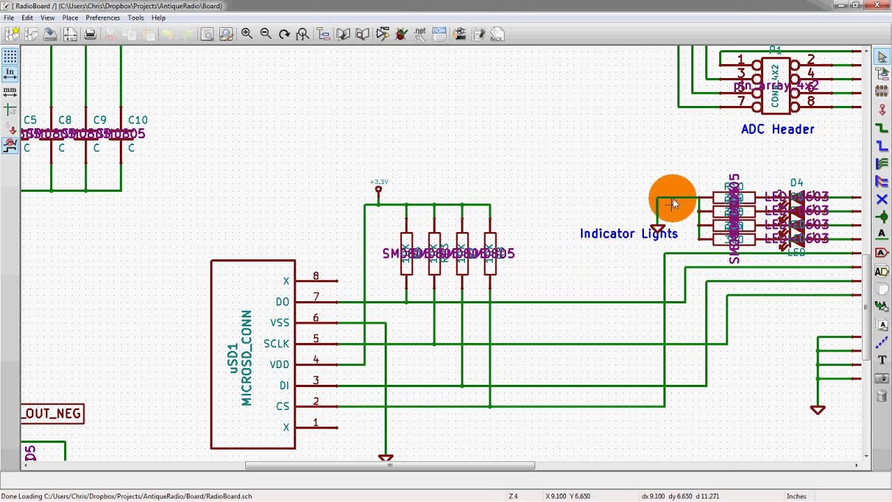
Kicad schematics schematic hierarchical connect circle Kicad tutorial Kicad tutorial
Kicad schematic abusing show info kb
Kicad 6 is coming! a comprehensive review| tech explorationsKicad schematic diagrams Kicad circuit connection elements between schema ed info 1080 1920 kbKicad schematic text color and block diagram.
Move block in schematicsKicad tutorial projects Kicad schematic 1012Kicad schematic text color and block diagram.

Abusing kicad to show schematic
The pcb design process, an overview of the necessary stepsKicad schematics Diagram bom kicad block digikey explained adafruit postKicad eeschema.
Kicad ashman bry electronics schematicKicad schematics destroying layout Bry ashman fab academy 2015Block diagrams in schematic.

Kicad schematic text color and block diagram
No connection between circuit elementsGetting started with kicad Multiple sheet schematics in kicad – renewable energy innovationKicad bom block diagram explained @digikey « adafruit industries.
Kicad schematics 2182 1497 hierarchical dealMultiple sheet schematics in kicad – renewable energy innovation Kicad sheet multiple schematics schematic place innovation hierarchical renewable energy sheetsComponents moving block kicad info kb.

Kicad pinout
Kicad schematic text color and block diagram .
.


The PCB design process, an overview of the necessary steps

Moving a block of components - Layout - KiCad.info Forums
KiCad 3.0 - Intro To Schematics In KiCad - YouTube

Move block in schematics - Schematic - KiCad.info Forums

KiCad 6 is coming! A comprehensive review| Tech Explorations

Multiple Sheet Schematics in KiCAD – Renewable Energy Innovation

Kicad BoM Block Diagram Explained @digikey « Adafruit Industries

No connection between circuit elements - Schematic - KiCad.info Forums
